- 您现在的位置:买卖IC网 > Sheet目录1991 > CS4361-CZZR (Cirrus Logic Inc)IC DAC STER 6CH 105DB 20-TSSOP
8
CS4361
Confidential Draft
9/30/11
DIGITAL INPUT CHARACTERISTICS
6.
RST pin has an input threshold relative to VL, but is VA tolerant.
7.
Iin for LRCK is ±20 A max.
POWER & THERMAL CHARACTERISTICS
8.
Current consumption increases with increasing FS and increasing MCLK. Typ and Max values are
based on highest FS and highest MCLK. Current variance between speed modes is small.
9.
Power-Down Mode is defined when all clock and data lines are held static.
10. Valid with the recommended capacitor values on VQ and FILT+ as shown in the typical connection di-
agram in Section 4.
Parameters
Symbol
Min
Typ
Max
Units
High-Level Input Voltage -all input Pins except RST (% of VL)
VIH
70%
-
V
Low-Level Input Voltage -all input Pins except RST (% of VL)
VIL
-
30%
V
High-Level Input Voltage -RST pin (Note 6)
(% of VL)
VIH
90%
-
V
Low-Level Input Voltage -RST pin
(% of VL)
VIL
-
10%
V
Input Leakage Current
Iin
--
±10
A
Input Capacitance
-
8
-
pF
Parameters
Symbol
5V Nom
Units
Min
Typ
Max
Power Supplies
Power Supply Current
normal operation
power-down state (Note 9)
IA
IL
IA
IL
-
66
0.1
300
26
90
1
-
mA
A
Power Dissipation
normal operation
power-down state (Note 9)
-
331
1.63
455
-
mW
Package Thermal Resistance
JA
-72
-
°C/Watt
Power Supply Rejection Ratio (Note 10)
(1 kHz)
(60 Hz)
PSRR
-
60
40
-
dB
AO U Tx
AG N D
3.3 F
V
out
R
L
C
L
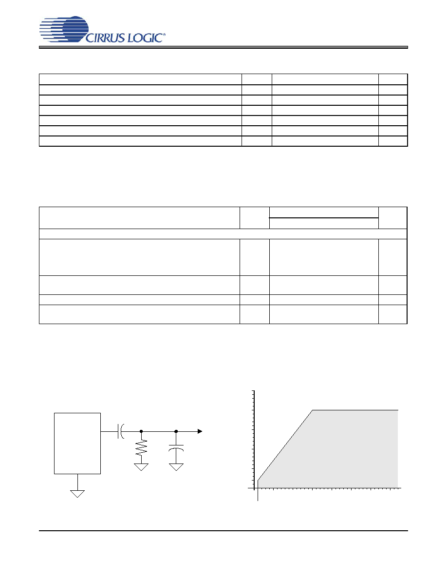
Figure 1. Equivalent Output Test Load
Figure 2. Maximum Loading
100
50
75
25
2.5
510
15
Safe Operating
Region
Cap
a
ci
ti
ve
L
o
a
d
--
C
(
p
F
)
L
Resistive Load -- R
(k
)
L
125
3
20
发布紧急采购,3分钟左右您将得到回复。
相关PDF资料
CS4362-KQZ
IC DAC 6CH 114DB 192KHZ 48LQFP
CS4362A-DQZ
IC DAC 6CH 114DB 192KHZ 48-LQFP
CS4364-CQZR
IC DAC 103DB 24BIT 6CH 48-LQFP
CS4382A-DQZ
IC DAC 8CH 114DB 192KHZ 48-LQFP
CS4384-CQZR
IC DAC 8CH 103DB 192KHZ 48-LQFP
CS4385-DQZR
IC DAC 8CH 114DB 192KHZ 48-LQFP
CS4391A-KZZR
IC DAC 24BIT 192KHZ W/VC 20TSSOP
CS4392-KZZ
IC DAC 24BIT 192KHZ W/VC 20TSSOP
相关代理商/技术参数
CS4361-DZZ
制造商:CIRRUS 制造商全称:Cirrus Logic 功能描述:20-pin, 24-bit, 192 kHz, 6-channel D/A Converter
CS4362
制造商:CIRRUS 制造商全称:Cirrus Logic 功能描述:114 dB, 192 kHz 6-Channel D/A Converter
CS4362_04
制造商:CIRRUS 制造商全称:Cirrus Logic 功能描述:114 dB, 192 kHz 6-channel D/A Converter
CS4362_08
制造商:CIRRUS 制造商全称:Cirrus Logic 功能描述:114 dB, 192 kHz 6-Channel D/A Converter
CS4362A
制造商:CIRRUS 制造商全称:Cirrus Logic 功能描述:114 dB, 192 kHz 6-Channel D/A Converter
CS4362A_08
制造商:CIRRUS 制造商全称:Cirrus Logic 功能描述:114 dB, 192 kHz 6-Channel D/A Converter
CS4362A_09
制造商:CIRRUS 制造商全称:Cirrus Logic 功能描述:114 dB, 192 kHz 6-Channel D/A Converter
CS4362A-CQZ
功能描述:音频数/模转换器 IC 6-Ch DAC 24-Bit 192kHz 114dB w/DSD RoHS:否 制造商:Texas Instruments 转换器数量: 分辨率:16 bit 接口类型:I2S, UBS 转换速率: 信噪比:98 dB 工作电源电压:5 V DAC 输出端数量:2 工作温度范围:- 25 C to + 85 C 电源电流:23 mA 安装风格:SMD/SMT 封装 / 箱体:TQFP-32 封装:Reel